



Build Your Custom Market Intelligence Report
Customize Your ReportKey Highlights
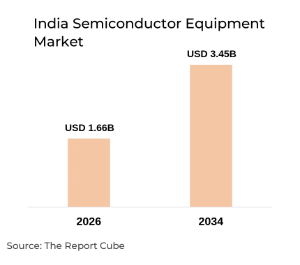
- The India Semiconductor Equipment Market was valued at USD 1,656.7 million in 2026, up about 8.97% from USD 1,520.3 million in 2025.
- Market size is projected to reach USD 3,446.2 million by 2034, an analyst extension of the published USD 3,144.3 million forecast for 2033.
- The market is forecast to grow at a CAGR of 9.59% during 2026-2034.
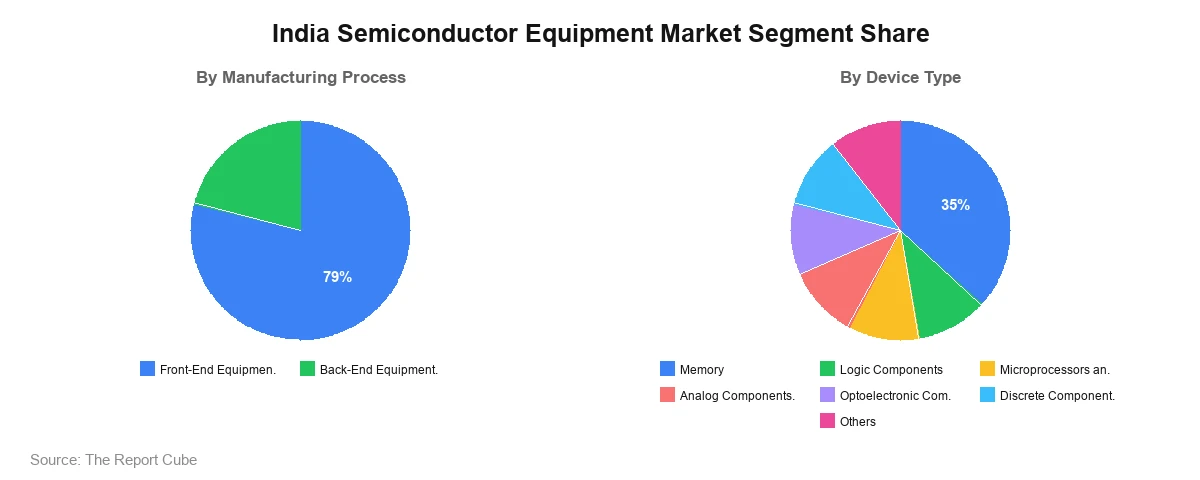
- By manufacturing process, front-end equipment led with a 79.8% share in 2025 and is also identified as the fastest-growing process segment.
- Gujarat is the largest state market, with a 35% share in 2025
- Government-backed semiconductor manufacturing investments, including ten approved projects worth about ₹1.6 lakh crore, are the major growth driver.
- Applied Materials, Lam Research, ASML, Tokyo Electron and KLA are expanding their engineering and customer-support activities in India.
Market Outlook
Semiconductor equipment covers the machinery used to fabricate wafers and to assemble, package, inspect and test chips. The India Semiconductor Equipment Market is relevant because the country is moving from chip consumption toward domestic manufacturing, and every fab, assembly and test facility needs a large installed base of specialised tools.
Demand currently comes from approved fabrication, assembly, testing, marking and packaging projects, along with pilot lines. Core product groups include lithography, deposition, etching, cleaning, metrology, bonding, dicing and automated test equipment. Procurement is tied to project construction, tool installation and process qualification, so demand follows project timelines rather than steady consumption.
The market was USD 1,656.7 million in 2026 and is projected to reach USD 3,446.2 million by 2034, a CAGR of 9.59%. Growth is supported by policy incentives, rising domestic electronics demand and global supplier engagement. Published estimates differ by publisher because of varying definitions, so this report uses as its benchmark.
Competition is led by international suppliers, as India has no established domestic equipment manufacturing base. Opportunities lie in servicing, localised components and advanced packaging. Future direction depends on how quickly approved projects reach commercial production and on the pace of equipment procurement, commissioning and workforce development.
Government Regulations
The Semicon India Programme, approved in December 2021 with an outlay of ₹76,000 crore, supports semiconductor fabs, compound semiconductors, packaging, testing and design. The India Semiconductor Mission administers approvals under the Ministry of Electronics and Information Technology. The Government of India’s February 2026 update reported ten approved projects with envisaged investment of about ₹1.6 lakh crore, and India Semiconductor Mission 2.0 was announced in February 2026 with greater emphasis on equipment, materials and ecosystem development. Approved projects in Gujarat, Assam, Uttar Pradesh, Odisha and Andhra Pradesh create demand for tools, installation and process qualification. NITI Aayog has noted that about 90-95% of India’s semiconductor and component needs were imported as of 2023, reinforcing the policy focus on domestic manufacturing. For equipment suppliers, incentives improve project viability, while approval timelines and local-support expectations shape procurement.
India Semiconductor Equipment Market Dynamics
Market dynamics are shaped by government project approvals, import dependence, the build-out of fabrication and packaging capacity, and supplier localisation. Capital intensity, infrastructure readiness and skilled-workforce availability influence how quickly announced investments convert into equipment orders in the India Semiconductor Equipment Market.
|
Factor |
Type |
Specific Impact on Market |
Magnitude |
|---|---|---|---|
|
Semicon India Programme and approved projects |
Driver |
Creates a pipeline of fab, OSAT and ATMP equipment demand |
High |
|
Domestic demand and import dependence |
Driver |
Supports the case for local manufacturing and tool procurement |
Medium-High |
|
Localisation of equipment components and servicing |
Opportunity |
Opens room for Indian engineering and support firms |
Medium |
|
High capital cost and technology dependence |
Challenge |
Raises project costs and relies on imported advanced tools |
High |
|
Infrastructure and skilled workforce constraints |
Challenge |
Can delay commissioning and equipment utilisation |
Medium-High |
|
Advanced packaging expansion |
Trend |
Increases demand for bonding, inspection and test tools |
Medium-High |
Growth Drivers
Government-backed manufacturing investments: The Semicon India Programme has created a policy framework for fabrication, compound semiconductor, packaging and testing projects. The February 2026 update reported ten approved projects with envisaged investment of about ₹1.6 lakh crore. Higher capital investment in facilities increases demand for wafer processing, packaging, inspection and test equipment, as well as installation and qualification services.
Rising domestic demand and import dependence: NITI Aayog reports that about 90-95% of India’s semiconductor and component requirements were met through imports as of 2023. Automotive, telecom, consumer, industrial and data-centre demand for chips strengthens the rationale for local production. Expansion of domestic manufacturing is expected to generate fabrication, packaging and testing equipment demand and support a local supply chain.
Market Opportunities
Equipment component localisation: India can develop capabilities in subsystems, precision engineering, automation, motion control and vacuum systems. India Semiconductor Mission 2.0 places greater emphasis on domestic equipment and materials capabilities. This gives Indian engineering firms an opportunity to join global equipment supply chains while reducing dependence on imported parts and lowering lifecycle costs for fabs and packaging facilities operating in the country.
Servicing, maintenance and testing infrastructure: A growing installed base requires installation, commissioning, preventive maintenance, calibration, spare parts and process monitoring. Providers with local technical support and training capabilities can benefit as facilities scale. Automated testing and inspection solutions also gain relevance as assembly and test capacity expands, creating recurring service revenue beyond initial tool sales for suppliers with a presence in India.
Industry Challenges
High capital expenditure and technology dependence: Equipment acquisition involves heavy spending, complex engineering and long implementation periods. India relies on established international manufacturers for lithography, deposition, etching, inspection and test systems. NITI Aayog has flagged import reliance as a structural weakness. High costs and technology-transfer requirements can raise project budgets and delay capacity expansion in the India Semiconductor Equipment Market.
Infrastructure and skilled workforce constraints: Fabs need reliable electricity, specialised water treatment, contamination-controlled environments and trained personnel, including process engineers, maintenance specialists and automation professionals. The government has included talent development and research infrastructure within its ecosystem priorities. Gaps in infrastructure readiness or workforce availability can influence commissioning schedules, equipment utilisation and the pace at which approved projects translate into procurement.
Need Specific Data, Let’s Customize the Report for You
Request CustomizationMarket Trends
Expansion of advanced packaging: Government-supported OSAT, ATMP and compound semiconductor projects are creating opportunities for packaging, bonding, inspection and test equipment. The Tata Electronics and Tokyo Electron partnership, announced in September 2024, illustrates the integration of front-end fabrication with back-end assembly and test infrastructure. Advanced packaging is becoming a larger part of India’s manufacturing strategy and tool demand.
Growing presence of global equipment suppliers: Applied Materials has set up an India Validation Center, Lam Research has begun a Bengaluru systems laboratory, Tokyo Electron has a Bengaluru development site, and ASML has an agreement with Tata Electronics. These moves show India emerging as an engineering and technology development location, not only an equipment consumption market, and deepen customer-support capability.
India Semiconductor Equipment Market Segment Analysis
The market is segmented by manufacturing process, equipment type, technology, device type and end user. Segmentation reflects how equipment is purchased across fabrication, assembly, packaging and testing, and each category is analysed independently without combining shares across dimensions.
By Manufacturing Process
- Front-End Equipment
- Back-End Equipment
Front-end equipment leads with a 79% share in 2025 and is also identified as the fastest-growing process segment. It covers lithography, deposition, etching, cleaning, planarisation and metrology tools, which carry high unit values and underpin wafer fabrication. Back-end equipment, covering assembly, packaging and testing tools, held 20.2% and gains importance as India’s approved pipeline contains many OSAT and ATMP projects. P&S Intelligence reports a different split (60% front-end, 40% back-end), so the shares are not averaged.
By Device Type
- Memory
- Logic Components
- Microprocessors and Microcontrollers
- Analog Components
- Optoelectronic Components
- Discrete Components
- Others
Memory is the largest device category, with a 35% share in 2025, supported by memory assembly and test projects such as Micron’s facility in Sanand, Gujarat. Logic components are identified as the fastest-growing category, driven by fabrication projects and demand from AI, data centres and electronics. This is a demand-side classification, not a share of each equipment category. Microprocessors, analog, optoelectronic and discrete components remain established or specialised.
India Semiconductor Equipment Market Regional Analysis
India’s equipment demand is concentrated where approved semiconductor projects are located, led by Gujarat in the west and supported by southern, northern and eastern clusters. Only one state-level share is published, from P&S Intelligence for 2025, so other regional shares are not estimated.
|
Region |
Estimated Market Share |
Key Growth Factors |
Industry Trends |
|---|---|---|---|
|
West India |
Gujarat: 35% (2025) |
Tata Electronics fab at Dholera; Micron, CG Power and Kaynes projects in Sanand |
Fab and ATMP/OSAT concentration |
|
South India |
- |
Engineering centres in Bengaluru; Karnataka identified as fastest-growing state |
R&D, validation and development hubs |
|
North India |
- |
Uttar Pradesh project at Jewar |
Emerging semiconductor manufacturing |
|
East and Northeast India |
- |
Tata OSAT in Assam; compound semiconductor and packaging projects in Odisha |
Packaging and compound semiconductors |
|
Rest of India |
- |
Other locations |
Not disclosed |
West India: Gujarat is the largest state market at 35% in 2025, supported by Tata Electronics’ Dholera fab and assembly and test projects by Micron, CG Power and Kaynes in Sanand. The concentration of front-end and back-end projects in one state drives procurement of both fabrication and packaging tools, and the state’s share reflects projects moving toward equipment procurement.
Competitive Landscape
The market is served mainly by international equipment manufacturers with strong technology positions in wafer fabrication, inspection and testing. India is an emerging manufacturing location, so global suppliers are building engineering, validation and support capabilities locally. The companies below are relevant participants, not a verified ranking of Indian market share.
|
Company |
Competitive Strength |
Primary Segment Served |
|---|---|---|
|
Applied Materials |
Deposition, etch, materials engineering, inspection and process control |
Front-end equipment |
|
Lam Research |
Etching, deposition, photoresist stripping and wafer cleaning |
Front-end equipment |
|
ASML |
Advanced lithography systems |
Front-end equipment |
|
Tokyo Electron |
Wafer processing, coating, developing and cleaning systems |
Front-end and fab/packaging infrastructure |
|
KLA Corporation |
Inspection, metrology and process control |
Front-end equipment |
|
Advantest |
Automated test equipment |
Back-end testing |
|
SCREEN Holdings |
Wafer cleaning and processing |
Front-end equipment |
|
Cohu |
Test handlers and test systems |
Back-end testing |
Applied Materials: The United States-based company supplies deposition, etch, materials engineering, inspection and process control systems. It has a presence in Bengaluru, Chennai, Mumbai and Pune, and has established an India Validation Center with 300mm wafer R&D capabilities, along with a collaborative engineering centre announced for Bengaluru. Its competitive position rests on equipment engineering and process development strength.
Tokyo Electron: The Japan-based company offers wafer processing, coating, developing, cleaning and semiconductor production systems. In September 2024 it partnered with Tata Electronics to support the Dholera fab and the Assam assembly and test facility, and it opened a Bengaluru development site in September 2025. Its broad portfolio and Tata relationship position it across both fabrication and packaging.
Recent Developments and Updates
- May 2026: Tata Electronics and ASML signed an agreement to support the Dholera semiconductor fab, as reported by the Press Information Bureau. The agreement links advanced lithography supply to India’s first planned commercial fab.
- February 2026: The Government of India announced India Semiconductor Mission 2.0 and reported ten approved projects with envisaged investment of about ₹1.6 lakh crore, placing greater focus on equipment, materials and ecosystem development.
- September 2025: Tokyo Electron established a development site in Bengaluru, following its 2024 partnership with Tata Electronics. The move strengthens local engineering and customer support for fab and assembly infrastructure.
India Semiconductor Equipment Market Future Outlook
The India Semiconductor Equipment Market is expected to expand from USD 1,656.7 million in 2026 to USD 3,446.2 million by 2034 at a CAGR of 9.59%. Growth should move from initial fab and OSAT tool procurement toward broader demand for testing, inspection, process control and servicing. Advanced packaging, compound semiconductors and 3D technologies offer further opportunities. The 2034 value is an analyst extension of the published 2033 forecast, not an independently published figure.
Competition will likely centre on global suppliers deepening local engineering, validation and support operations, while Indian firms target components and services. Risks include project delays, high capital costs, import dependence, infrastructure readiness and workforce shortages. Actual procurement may shift between years if fab construction or commercial production schedules move, so long-term growth depends on converting approved projects into operating facilities.
India Semiconductor Equipment Market Report Coverage
This India Semiconductor Equipment Market report summarises market size, forecast assumptions, segmentation, regional context and the competitive landscape using supplied inputs and cited research.
|
Parameter |
Details |
|---|---|
|
Market Name |
India Semiconductor Equipment Market |
|
Market Size (Base Year) |
USD 1,656.7 million (2026) |
|
Market Size (Forecast Year) |
USD 3,446.2 million (2034) |
|
CAGR |
9.59% (2026-2034) |
|
Base Year |
2026 |
|
Historical Period |
2021-2025 |
|
Forecast Period |
2026-2034 |
|
Geographic Scope |
India |
|
Segmentation |
By Manufacturing Process; By Equipment Type; By Technology; By Device Type; By End User |
|
Regions Covered |
West India, South India, North India, East and Northeast India, Rest of India |
|
Key Companies |
Applied Materials; Lam Research; ASML; Tokyo Electron; KLA Corporation; Advantest; SCREEN Holdings; Cohu |
|
Customization |
Available as per requirement |
Why Choose This India Semiconductor Equipment Market Report?
- Presents the 2026 base value, 2034 forecast and 9.59% CAGR with stated sourcing and assumptions.
- Segments the market by manufacturing process, equipment type, technology, device type and end user.
- Explains market dynamics, including drivers, challenges, trends and the semiconductor policy environment.
- Provides regional context across West, South, North, East and Northeast India, with undisclosed shares identified.
- Profiles key global suppliers by capability and primary segment served.
- Identifies opportunities in advanced packaging, localisation, servicing and testing infrastructure.
- Supports investment, sourcing and market-entry decisions with clearly labelled estimates and limitations.
Table of Contents
Introduction
-
Objective of the Study
-
Product Definition
-
Market Segmentation
-
Study Variables
1. Research Methodology
-
Secondary Data Points
-
Companies Interviewed
-
-
Primary Data Points
-
Breakdown of Primary Interviews
-
2. Executive Summary
3. Market Dynamics
-
Market Drivers
-
Market Challenges
-
Opportunity Assessment
4. Recent Trends and Developments
5. Policy and Regulatory Landscape
6. India Semiconductor Equipment Market Overview and Forecast Analysis (2021–2034)
-
Market Size, By Value (USD Million)
-
Market Growth Rate (CAGR)
-
Historical Market Size and Annual Growth Analysis (2021–2025)
-
Market Forecast Analysis (2026–2034)
-
Demand–Supply Trends
-
Market Share, By Manufacturing Process
-
Front-End Equipment
-
Back-End Equipment
-
-
Market Share, By Equipment Type
-
Lithography Equipment
-
Deposition Equipment
-
Etching Equipment
-
Wafer Cleaning Equipment
-
Wafer Surface Conditioning Equipment
-
Inspection and Metrology Equipment
-
Ion Implantation and Thermal Processing Equipment
-
Assembly and Packaging Equipment
-
Dicing and Bonding Equipment
-
Semiconductor Testing Equipment
-
Wafer Handling and Automation Equipment
-
Others
-
-
Market Share, By Technology
-
2D
-
2.5D
-
3D
-
-
Market Share, By Device Type
-
Memory
-
Logic Components
-
Microprocessors and Microcontrollers
-
Analog Components
-
Optoelectronic Components
-
Discrete Components
-
Others
-
-
Market Share, By End User
-
Semiconductor Foundries
-
Integrated Device Manufacturers (IDMs)
-
Outsourced Semiconductor Assembly and Test (OSAT) Companies
-
Assembly, Testing, Marking and Packaging (ATMP) Companies
-
Research and Pilot Manufacturing Facilities
-
-
Market Share, By Region
-
West India
-
South India
-
North India
-
East and Northeast India
-
Rest of India
-
-
Market Share, By Competitors
-
Competition Characteristics
-
Revenue Shares
-
7. Lithography Equipment India Semiconductor Equipment Market Overview, 2021–2034F
-
Market Size, By Value (USD Million)
-
Market Forecast and Growth Analysis
-
Market Segmentation, By Technology
-
Extreme Ultraviolet (EUV) Lithography
-
Deep Ultraviolet (DUV) Lithography
-
8. Deposition Equipment India Semiconductor Equipment Market Overview, 2021–2034F
-
Market Size, By Value (USD Million)
-
Market Forecast and Growth Analysis
-
Market Segmentation, By Technology
-
Chemical Vapor Deposition (CVD)
-
Physical Vapor Deposition (PVD)
-
Atomic Layer Deposition (ALD)
-
Epitaxy Equipment
-
9. Etching Equipment India Semiconductor Equipment Market Overview, 2021–2034F
-
Market Size, By Value (USD Million)
-
Market Forecast and Growth Analysis
-
Market Segmentation, By Technology
-
Plasma Etching Equipment
-
Wet Chemical Etching Equipment
-
Dry Etching Equipment
-
10. Wafer Cleaning Equipment India Semiconductor Equipment Market Overview, 2021–2034F
-
Market Size, By Value (USD Million)
-
Market Forecast and Growth Analysis
-
Market Segmentation, By Type
-
Single-Wafer Cleaning Systems
-
Batch Cleaning Systems
-
Scrubber Systems
-
11. Inspection and Metrology Equipment India Semiconductor Equipment Market Overview, 2021–2034F
-
Market Size, By Value (USD Million)
-
Market Forecast and Growth Analysis
-
Market Segmentation, By Type
-
Defect Inspection Systems
-
Critical Dimension Metrology
-
Film Thickness Measurement Systems
-
12. Assembly and Packaging Equipment India Semiconductor Equipment Market Overview, 2021–2034F
-
Market Size, By Value (USD Million)
-
Market Forecast and Growth Analysis
-
Market Segmentation, By Type
-
Die Attach Equipment
-
Wire Bonding Equipment
-
Flip-Chip Bonding Equipment
-
Thermocompression Bonding Equipment
-
Encapsulation and Molding Equipment
-
Advanced Packaging Equipment
-
13. Semiconductor Testing Equipment India Semiconductor Equipment Market Overview, 2021–2034F
-
Market Size, By Value (USD Million)
-
Market Forecast and Growth Analysis
-
Market Segmentation, By Type
-
Wafer-Level Testing Equipment
-
Final IC Testing Equipment
-
Automated Test Equipment (ATE)
-
Burn-In and Reliability Testing Equipment
-
Test Handlers and Wafer Probers
-
14. Competitive Outlook (Company Profiles – Partial List)
14.1 Applied Materials Inc.
-
Company Overview
-
Business Segments
-
Semiconductor Equipment Product Portfolio
-
India Business Presence
-
Strategic Alliances / Partnerships
-
Recent Developments
14.2 ASML Holding N.V.
-
Company Overview
-
Business Segments
-
Semiconductor Equipment Product Portfolio
-
India Business Presence
-
Strategic Alliances / Partnerships
-
Recent Developments
14.3 Lam Research Corporation
-
Company Overview
-
Business Segments
-
Semiconductor Equipment Product Portfolio
-
India Business Presence
-
Strategic Alliances / Partnerships
-
Recent Developments
14.4 Tokyo Electron Limited
-
Company Overview
-
Business Segments
-
Semiconductor Equipment Product Portfolio
-
India Business Presence
-
Strategic Alliances / Partnerships
-
Recent Developments
14.5 KLA Corporation
-
Company Overview
-
Business Segments
-
Semiconductor Equipment Product Portfolio
-
India Business Presence
-
Strategic Alliances / Partnerships
-
Recent Developments
14.6 SCREEN Holdings Co. Ltd.
-
Company Overview
-
Business Segments
-
Semiconductor Equipment Product Portfolio
-
India Business Presence
-
Strategic Alliances / Partnerships
-
Recent Developments
14.7 ASM International N.V.
-
Company Overview
-
Business Segments
-
Semiconductor Equipment Product Portfolio
-
India Business Presence
-
Strategic Alliances / Partnerships
-
Recent Developments
14.8 Hitachi High-Tech Corporation
-
Company Overview
-
Business Segments
-
Semiconductor Equipment Product Portfolio
-
India Business Presence
-
Strategic Alliances / Partnerships
-
Recent Developments
14.9 Canon Inc.
-
Company Overview
-
Business Segments
-
Semiconductor Equipment Product Portfolio
-
India Business Presence
-
Strategic Alliances / Partnerships
-
Recent Developments
14.10 Nikon Corporation
-
Company Overview
-
Business Segments
-
Semiconductor Equipment Product Portfolio
-
India Business Presence
-
Strategic Alliances / Partnerships
-
Recent Developments
15. Contact Us & Disclaimer
Top Key Players & Market Share Outlook
- Applied Materials Inc.
- ASML Holding N.V.
- Lam Research Corporation
- Tokyo Electron Limited
- KLA Corporation
- SCREEN Holdings Co. Ltd.
- ASM International N.V.
- Hitachi High-Tech Corporation
- Canon Inc.
- Nikon Corporation
Frequently Asked Questions